


Phoenix / Washington: Accelerating the ongoing re-shoring of critical microelectronics manufacturing, the U.S. Department of Commerce has finalized $45 billion in expanded federal grants, commercial debt facilities, and advanced R&D consortia funding under the CHIPS and Science Implementation Strategy.
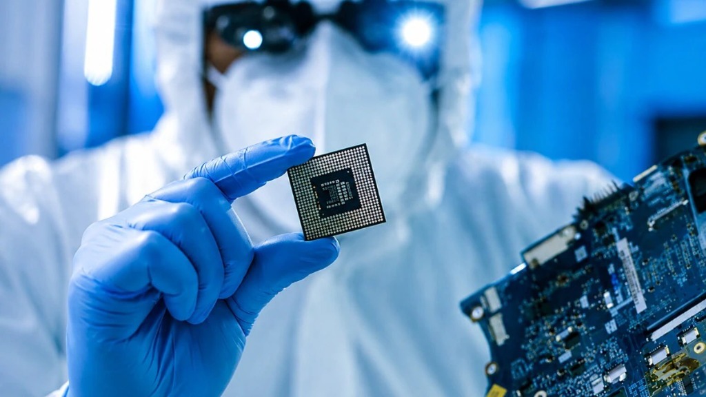
The initiative establishes the American Next-Gen Silicon Manufacturing Corridor, directly supporting the commercial installation of sub-2nm fabrication nodes, High-NA extreme ultraviolet (EUV) photolithography scanners, and high-density 3D wafer-level advanced packaging facilities across Arizona, Texas, and Ohio.
Securing Sovereign AI and Supercomputing Silicon
As artificial intelligence foundation models and hyperscale cloud networks demand exponential increases in compute density and thermal efficiency, securing domestic access to cutting-edge semiconductor lithography has become an urgent strategic priority for both economic competitiveness and national defense.
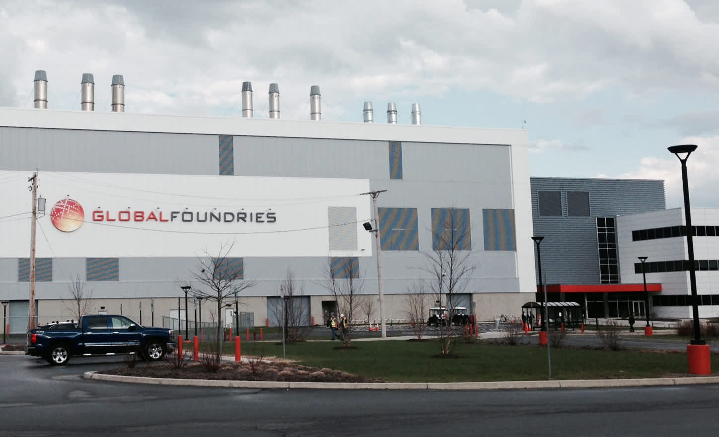
Under the new agreements, leading global foundry operators and domestic integrated device manufacturers will dedicate a minimum of forty percent of planned high-volume manufacturing lines in Columbus, Phoenix, and Sherman to domestic commercial AI accelerator and sovereign defense microelectronics contracts.
"American leadership in artificial intelligence and quantum computing cannot rest on fragile overseas fabrication ecosystems," stated the Secretary of Commerce during the formal announcement in Phoenix. "Today’s commitments guarantee that the world’s most sophisticated sub-2nm transistors are not only designed in America, but manufactured and packaged by American workers in state-of-the-art domestic facilities."
Advanced Packaging and Chemical Ecosystems
A major focus of the expanded corridor strategy is addressing the domestic bottleneck in advanced semiconductor packaging. The federal allocation directs $12 billion specifically toward commercializing glass substrate packaging, chiplet integration standards, and silicon photonics interconnects.
Additionally, thirty-five specialty chemical suppliers and substrate manufacturers have confirmed co-locating new purification and production plants adjacent to the primary fabrication clusters, creating over 22,000 high-skilled advanced manufacturing engineering jobs.
Workforce Development and University Partnerships
The federal framework mandates that $3 billion be channeled into regional microelectronics workforce development institutes. Partnering with twelve major state universities and technical colleges, the program will fund cleanroom apprenticeships, semiconductor engineering scholarships, and automated technician certification curriculums to meet the sector's long-term labor demand.
Commercial pilot wafer production at the new Arizona and Ohio sub-2nm facilities is on track to begin initial qualification runs by late 2026, with full-scale high-volume manufacturing scheduled for mid-2027.